Designing a Compact 150W OCL Amplifier (My High School Project)
Digging through my old hard drives, I found a project from my vocational high school days back in October 2018. It is a design for a 150W OCL (Output Capacitor-Less) Audio Amplifier.
I designed the schematic and PCB layout using Proteus 8. Since this board has been tested and works reliably, I decided to share it here as a design reference for anyone interested in DIY audio.
Understanding Audio Amplifiers (For Beginners)
Before we dive into the circuit, let’s briefly explain what an amplifier does.
Imagine you have a tiny stream of water (the audio signal from your phone or laptop). It’s too weak to turn a large water wheel (the speaker). An amplifier acts like a massive faucet: it uses the small stream to control a much larger flow of water from a reservoir (the power supply), creating a powerful force that can move the speaker cone and create sound.
Why OCL (Output Capacitor-Less)?
There are many classes of amplifiers (Class A, B, AB, D, etc.) and coupling methods. This specific design is an OCL Amplifier.
In older or simpler single-supply designs (OTL), a large capacitor is placed at the output to block DC voltage from reaching the speaker. In an OCL design, we use a symmetrical dual power supply (V+ and V-), which allows us to connect the output directly to the speaker without that capacitor.
Pros and Cons
- The Good: The frequency response is much better, especially in the low end (Bass), because there is no capacitor filtering the output.
- The Bad: It requires a more complex power supply (Transformer with a Center Tap), and if a transistor fails, DC voltage can leak to the speaker and potentially burn the coil.
My Opinion: Personally, I prefer the OCL architecture. The absence of the output capacitor makes the sound feel “punchier” and more authentic compared to capacitor-coupled amps.
The Schematic Design
The circuit is a classic 150W push-pull configuration utilizing the TIP3055 and TIP2955 as the main power transistors.
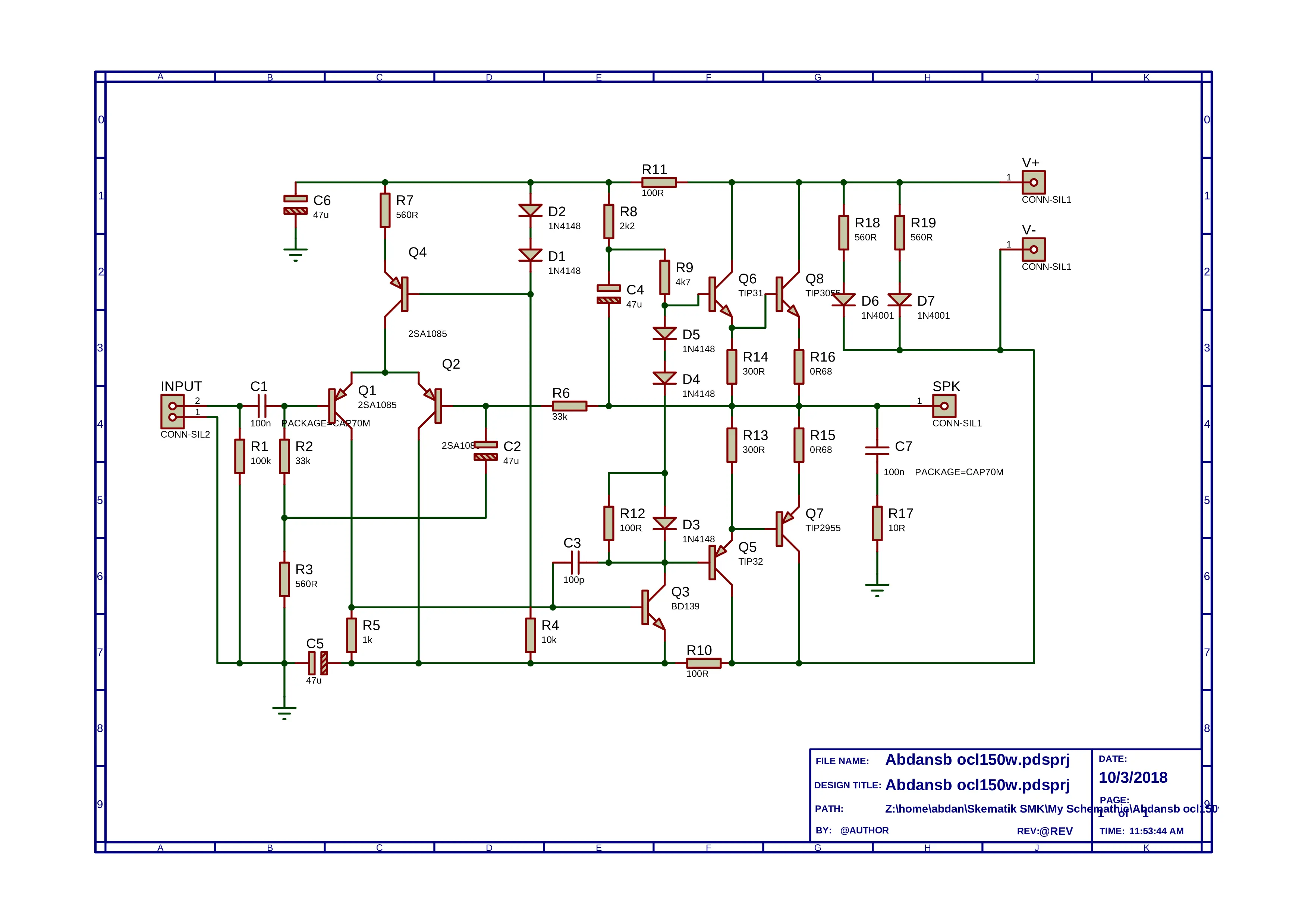 Figure 1: The full schematic captured in Proteus.
Key Components:
- Input Stage: A differential pair using 2SA1085 transistors to handle the input signal comparison.
- Drivers: The signal is amplified by BD139 and TIP31/TIP32 before hitting the final stage.
- Power Stage: The heavy lifting is done by the TIP3055 (NPN) and TIP2955 (PNP) pair.
The PCB Layout: A Compact Challenge
When I designed this layout in Proteus, my main goal was to make the PCB as small and compact as possible. I wanted a board that didn’t take up much space in an enclosure.
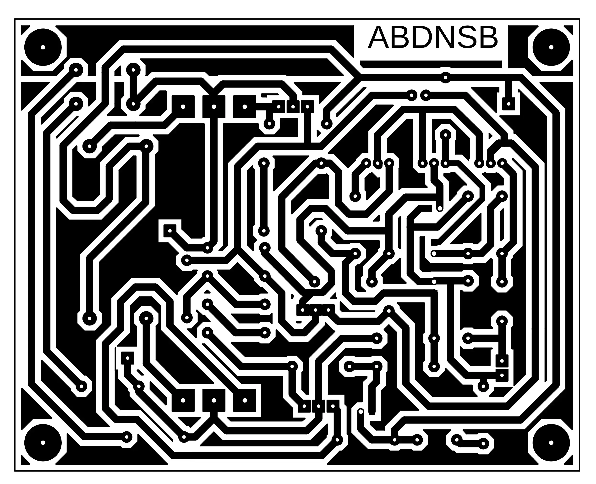 Figure 2: The bottom copper layer layout.
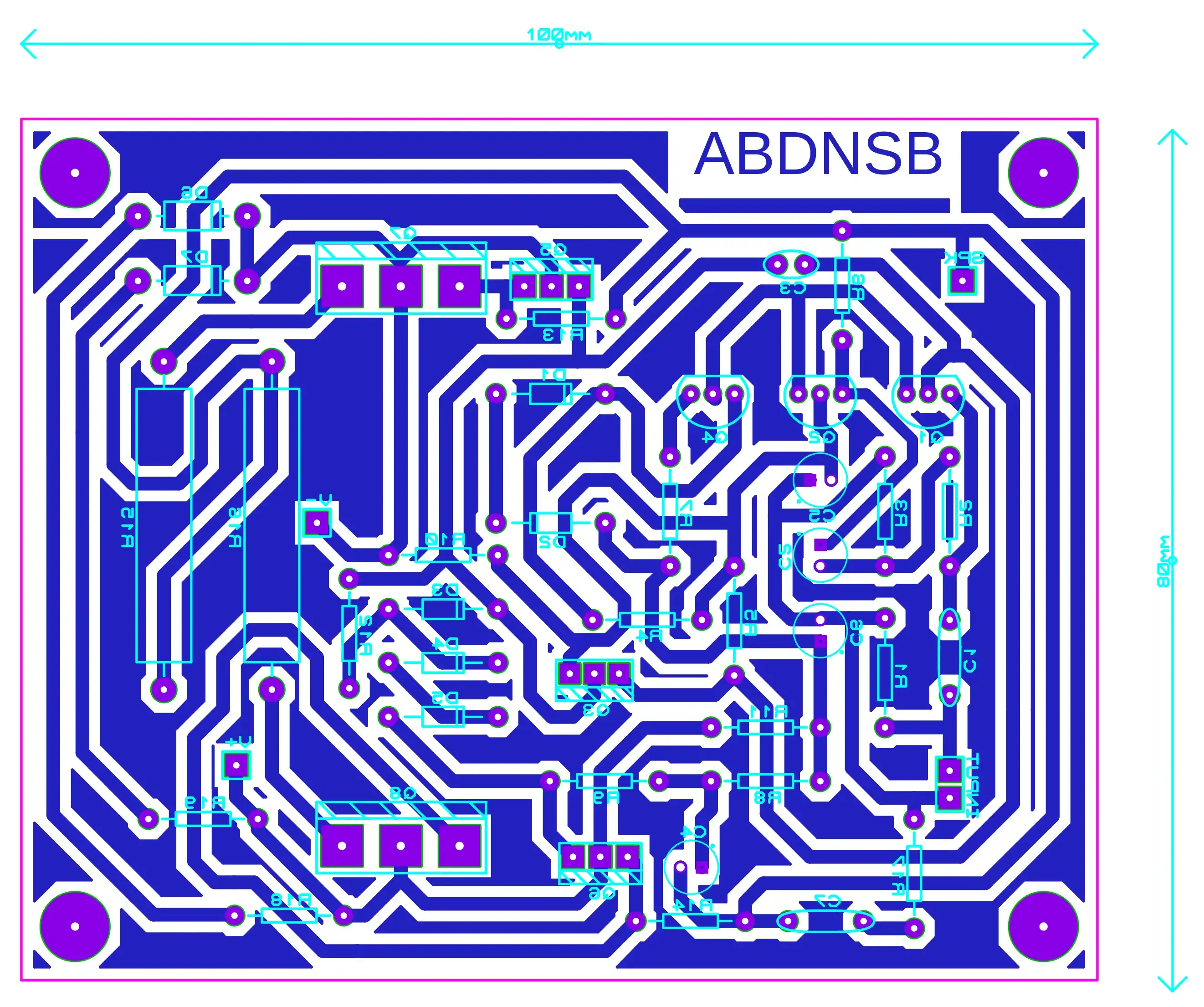 Figure 3: The component placement view.
The “Compact” Trade-off
While I succeeded in making the board small (approx 100mm x 80mm), there is a significant design trade-off you need to be aware of:
Warning: Because the PCB is so compact, the power transistors are placed very close to each other. You cannot mount a heatsink directly onto the PCB.
As you can see in the layout, the TO-220 and TO-3P packages are tightly packed. If you build this, you must mount the final transistors on an external heatsink and connect them to the PCB using wires. Do not try to run this amp without a heatsink, or the transistors will overheat instantly!
Conclusion
This project was a great learning experience during my vocational study. The routing has been verified, and the circuit is tested and functional—the traces are safe and handle the current well.
Feel free to use this layout for your own learning or modification. Just remember to wire those heatsinks properly!
Layout designed by ABDNSB. Original Schematic Date: 10/3/2018.