External VRM Mod Project Radeon HD6670
A hardware modification project to unlock the performance of an aging GPU by providing stable, adjustable voltage via an external Voltage Regulator Module (VRM).
Introduction
The MSI Radeon HD 6670 1GB GDDR5 is a mid-range graphics card from AMD’s Northern Islands generation. Key specifications relevant to this project include:
- GPU Core: Turks XT (40nm process)
- Stream Processors: 480
- Core Clock Speed: 800 MHz (stock)
- Memory Clock Speed: 1000 MHz (4.0 Gbps GDDR5 effective)
- Memory Interface: 128-bit
- TDP (Thermal Design Power): ~66W
- Power Connector: No external PCIe power connector (relies solely on PCIe slot power, 75W max)
- Cooling Solution: Single fan, heatsink assembly.
- VRM Configuration: Internal, typically 3 phase design for GPU and memory power delivery
These specs show how much the card relies on the PCIe slot for power, which limits how much i can overclock and boost performance. That’s why an external VRM mod is a pretty good idea. Also, the stock cooler is made for the 66W TDP, so i’ll need to keep an eye on it if i bump up the power.
Motivation
Why an External VRM?
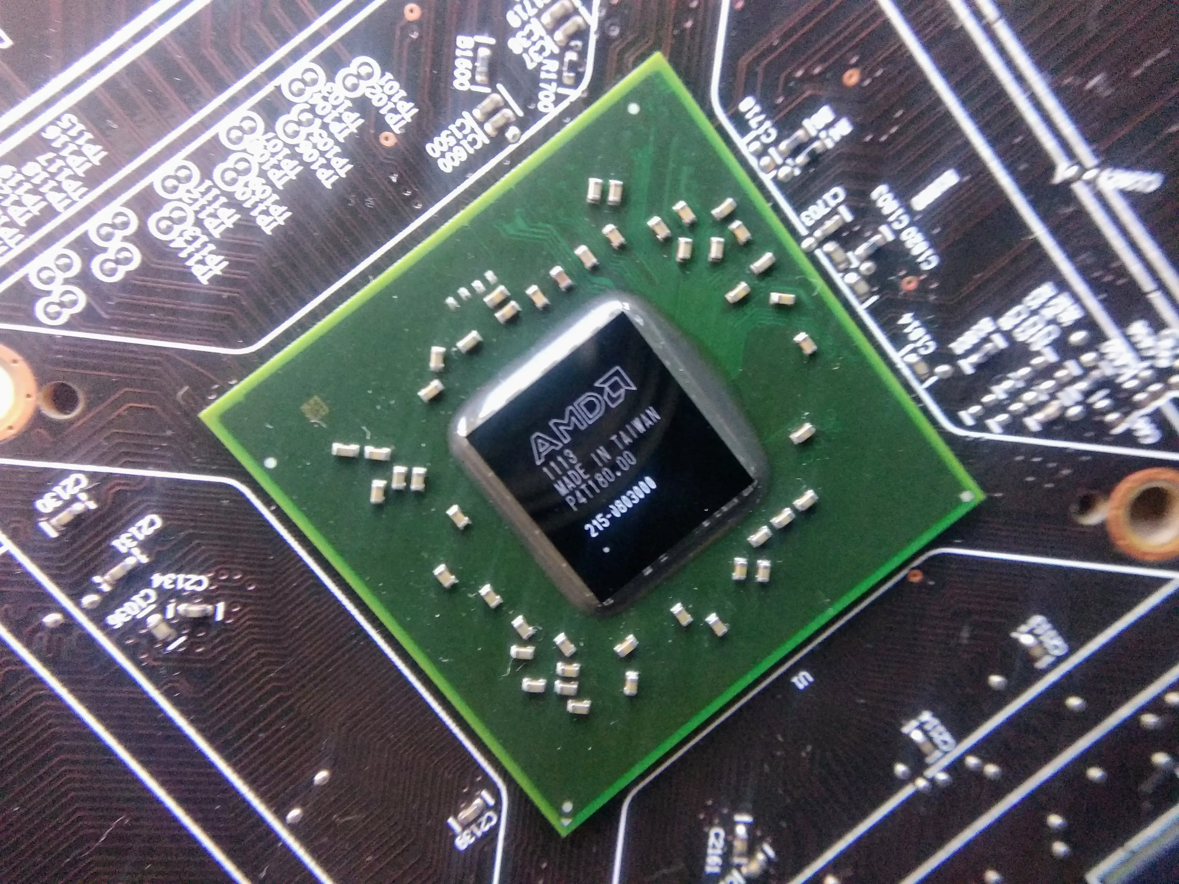
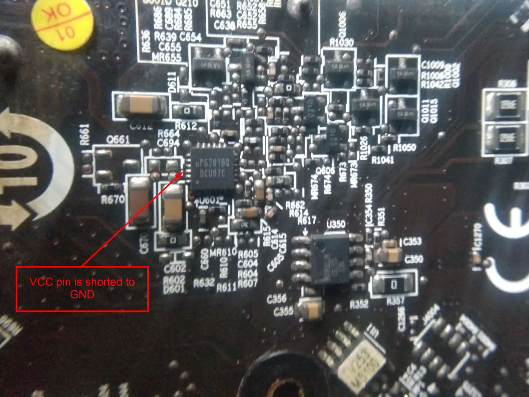
The power system on my MSI Radeon HD 6670 totally crapped out. Turns out the stock PWM controller, that little uP6201B chip, shorted. That’s the part that’s supposed to control the VRM MOSFETs and deliver the Vcore voltage to the GPU, so without it, the graphics card is basically a fancy paperweight.
Instead of trying to replace that tiny, surface-mounted chip – which would normally need a hot air station, and I only have a basic soldering iron – I decided to go a different route. I actually have another broken GPU with a perfectly good VRM section on it. So, the plan is to harvest that working VRM and integrate it with the MSI Radeon HD 6670. This way, I’m not just fixing the card. I’m also giving it a huge upgrade. The new VRM lets me control the voltage manually using hardware. This opens the door for real overclocking, something the stock card could never do.
Understanding the MSI Radeon HD 6670
The Voltage Regulator Modules (VRMs)
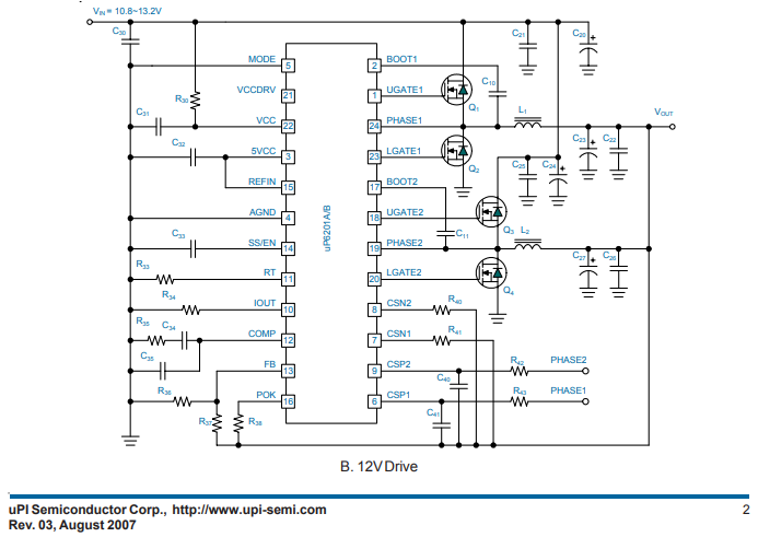
Figure 1: The official datasheet schematic for the uP6201B, a 2-phase synchronous buck controller which manages the GPU’s core voltage.
The GPU’s core voltage is supplied by a Voltage Regulator Module (VRM) that uses a 2-phase synchronous buck converter, managed by the uP6201B controller shown in Figure 1. A buck converter’s primary function is to step down a higher input voltage (e.g., 12V) to a much lower, precise output voltage (e.g., 1.0V for the GPU core).
Schematics Diagram
In a 2-phase design, the total power delivery is split between two identical circuits, or “phases,” which operate interleaved (180 degrees out of sync). This distributes heat, reduces electrical noise, and allows for a faster response to sudden changes in GPU load.
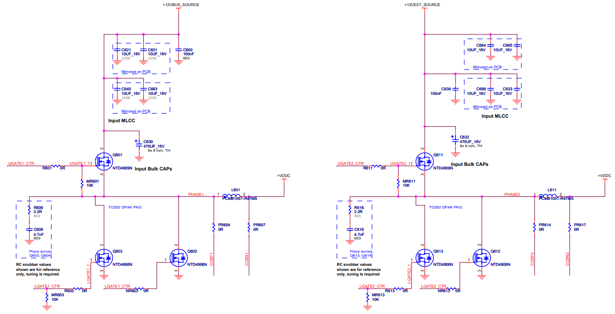
Figure 2: A 2-phase VRM reference schematic from a Radeon 6770, which is functionally identical to the circuit on the HD 6670.
To understand how the uP6201B is implemented, we can analyze the reference schematic. Although this diagram is from a Radeon 6770, the circuit topology and component numbering (e.g., Q801, L801) are virtually identical to the HD 6670 board.
This diagram illustrates a discrete 2-phase design. PHASE1 is designed with one high-side MOSFET (Q801) and has pads for two parallel low-side MOSFETs (Q802 and Q803). Using two low-side FETs is a common technique to handle higher current and distribute heat on more power-hungry GPUs. However, Q803 and Q813 are often optional. PHASE2 mirrors this design (Q811, Q812, Q813, and L811). The controller sends signals (like UGATE1_CTR from the uP6201B) to the gates of these MOSFETs, switching them on and off thousands of times per second to produce the final +VDDC (GPU core voltage).
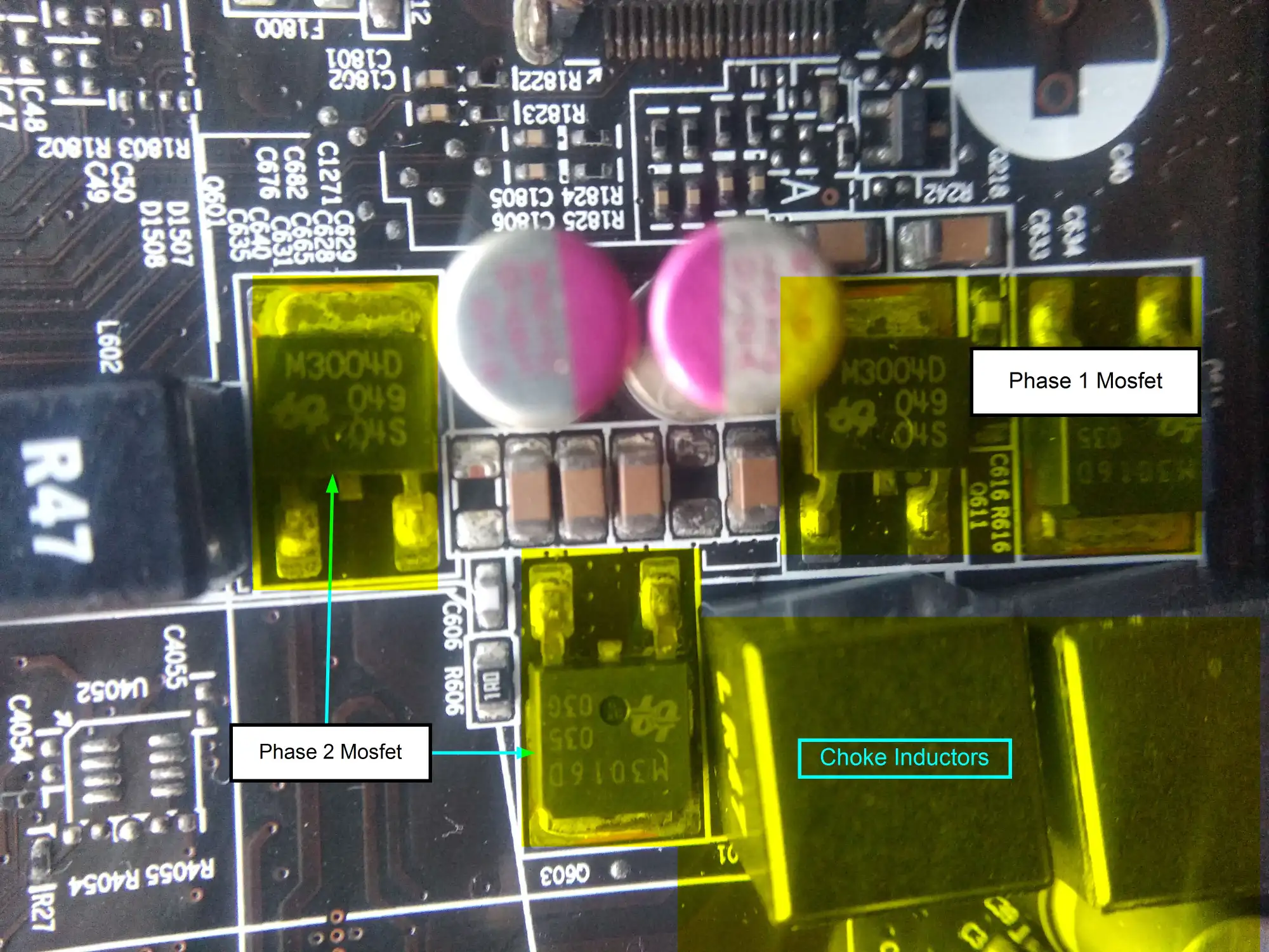
Figure 3: The physical 2-phase VRM circuit on the MSI Radeon HD 6670 PCB, showing a more integrated implementation.
On the actual MSI HD 6670 PCB, as shown in Figure 3, we see a more cost-effective and integrated version of this circuit. The pads for the secondary low-side MOSFETs (Q803, Q813 from the schematic) are not populated, as they are unnecessary for this card’s power target.
The “Choke Inductors” (L801/L811) are the next component in the power path.
These inductors are critical. Beyond storing energy, their internal resistance (DCR) is utilized by the uP6201B’s current sensing circuit to monitor the load. This current sense data, along with the main voltage feedback loop, is essential for the controller to operate correctly.
This inductors on the PCB are the connection points for the donor VRM. By cutting the traces immediately after these inductors and their associated output filter capacitors, the GPU core will be isolated from the original, faulty VRM. This allows the newly integrated external VRM to deliver power directly to the GPU, utilizing the existing filtering network while bypassing the defunct onboard power delivery system. This way ensures that the GPU receives clean, regulated voltage from the donor VRM without interference from the original, damaged circuit.
The Donor VRM From Asus Radeon R7 240 Low Profile
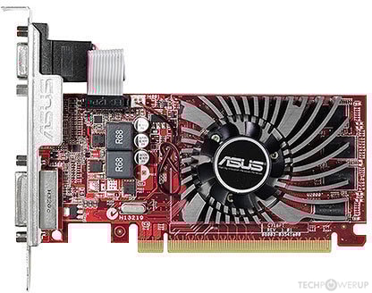
Figure 4: The donor card, an Asus Radeon R7 240 Low Profile (image courtesy of TechPowerUp).
For this project, the replacement voltage regulator module will be salvaged from a donor card, an Asus Radeon R7 240. This card was acquired in a non-functional state (due to a faulty GPU core) from a local marketplace for approximately $2 USD. While the GPU core is dead, its VRM section was tested and confirmed to be fully operational.
This card’s VRM design is fundamentally different from the target HD 6670. The MSI HD 6670 uses one controller IC (uP6201B) that is responsible for driving two phases simultaneously. In contrast, the Asus R7 240 uses two separate controller ICs (EM5305)—one for each phase.
Typical Application Circuit For The Controller
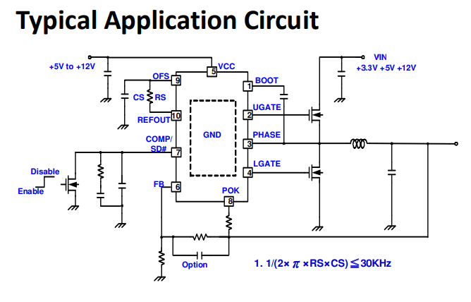
Figure 5: The typical application circuit for the EM5305, synchronous buck controller used on the R7 240.
The EM5305 is a dedicated single-phase synchronous buck controller.
Similar to the uP6201B, its job is to drive external MOSFETs. As shown in the diagram, the chip sends switching signals from its UGATE (Upper Gate) and LGATE (Lower Gate) pins to a pair of external N-Channel MOSFETs. These MOSFETs then feed the main power inductor and filter capacitors. The chip continuously monitors the output voltage via the Feedback (FB) pin and adjusts the switching of the MOSFETs to maintain a perfectly stable voltage.
The R7 240’s VRM simply consists of two complete copies of this circuit, side-by-side, working in parallel to share the load. This design choice was likely made due to the card’s low-profile form factor, as using two smaller, single-phase controllers allows for more flexible component placement on a cramped PCB.
Honestly, this two separate IC design offers significant advantages for repair and modification. It is much easier to troubleshoot because each phase is independent. If one phase fails, the fault can be isolated to a single EM5305 IC and its paired MOSFETs. The reduced pin count of the IC (as seen on the EM5305) also simplifies the probing and diagnosis process.
For my modification, I plan to physically cut the traces after the inductors and output filter capacitors to eliminate the rest of PCB. This step is important because the IC is designed to protect itself; if I cut the trace before the inductors, the IC will not output voltage. If the controller does not sense any current flowing from its circuit, it will register a fault condition (like an open circuit) and will shut down, outputting no voltage.
Hardware Components
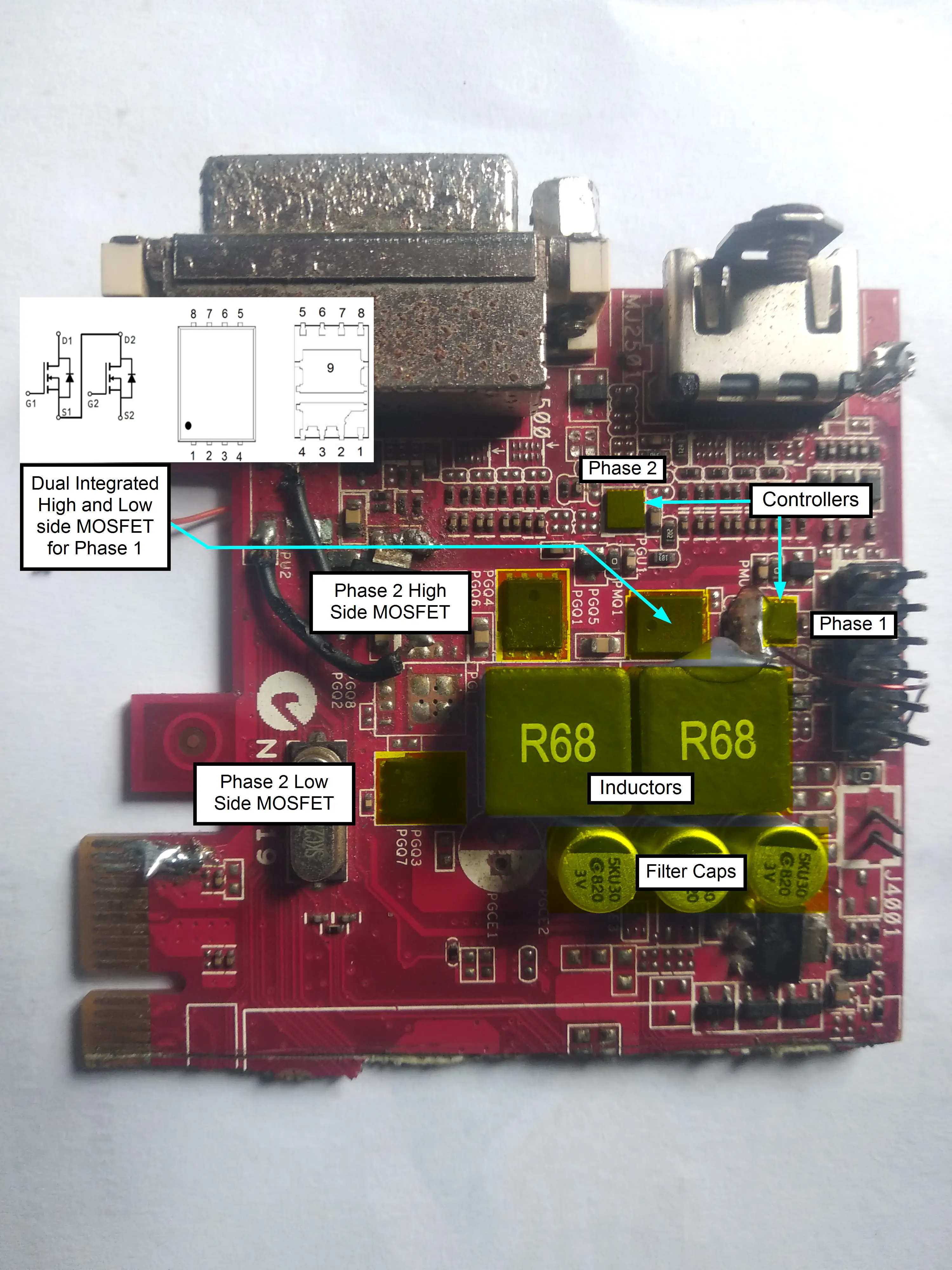
Figure 6: A detailed breakdown of the asymmetrical VRM components on the donor R7 240.
A closer examination of the donor card’s VRM, shown in Figure 6, reveals a unique and asymmetrical hardware implementation. At first glance, the circuit appears strange for a dual-phase system. A conventional discrete dual-phase VRM would typically use four main MOSFET packages (one high-side and one low-side for each of the two phases). However, as seen on the board, there are only three primary MOSFET packages visible.
The reason for this is a mix of integrated and discrete components, which are clearly labeled in Figure 6:
- Phase 1: This phase is highly integrated. As indicated by the label “Dual integrated High and Low side MOSFET for Phase 1,” it uses a single 8-pin SO-8 package. The diagram in Figure 6 clarifies this, showing that this single chip contains both the high-side and low-side N-Channel MOSFETs required for the phase. This “2-in-1” package is then driven by its dedicated “Controller” (the EM5305).
- Phase 2: This phase uses a more traditional, discrete approach. It is driven by its own “Controller” (the second EM5305) and uses two separate SO-8 packages: one “Phase 2 High Side MOSFET” and one “Phase 2 Low Side MOSFET.” As you’ve identified, these are M3052M series MOSFETs.
This hybrid or asymmetrical design (one integrated phase, one discrete phase) is another example of a clever space-saving technique, likely chosen to fit all the necessary components onto the constrained area of a low-profile PCB.
Comparative Analysis: Target VRM vs. Donor VRM
Before the modification could begin, a detailed comparison of the “Absolute Maximum Ratings” of both the original (target) and donor VRM components was necessary. This step is critical to ensure that the donor VRM is not a significant downgrade and can safely handle the power requirements of the HD 6670 GPU core.
Target VRM (HD 6670) Specifications
- Controller: 1x uPI Group uP6201 (2-Phase)
- Power Stages (Symmetrical):
- High-Side MOSFET: 1x M3004D (per phase)
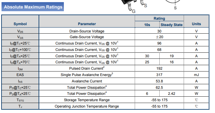
- Low-Side MOSFET: 1x M3016D (per phase)
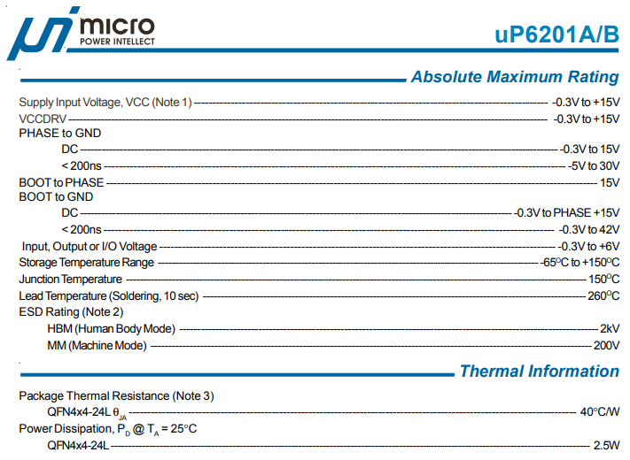
Figure 7: Absolute Maximum Ratings for the uP6201B Controller.
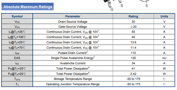
Figure 8: Absolute Maximum Ratings for the M3004D High-Side MOSFET.
Donor VRM (R7 240) Specifications
Controllers: 2x Excelliance MOS EM5305 (1-Phase) Power Stages (Asymmetrical):
- Phase 1: 1x Niko-Sem P0903YK (Dual N-Channel)
- Phase 2: 1x M3052M (High-Side) & 1x M3058M (Low-Side)
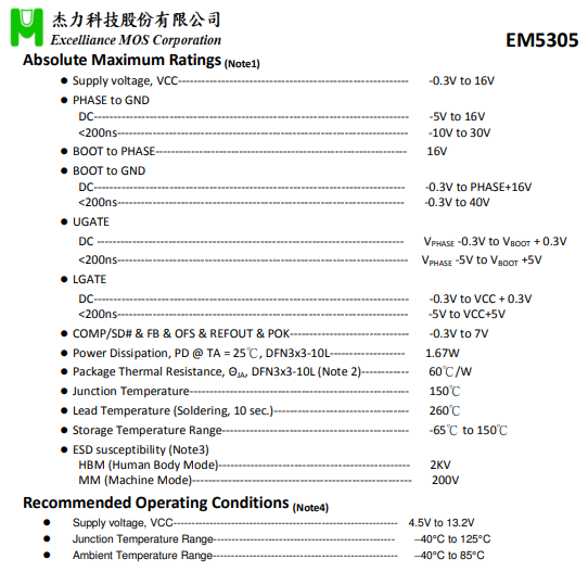
Figure 10: Absolute Maximum Ratings for the EM5305 Controller.
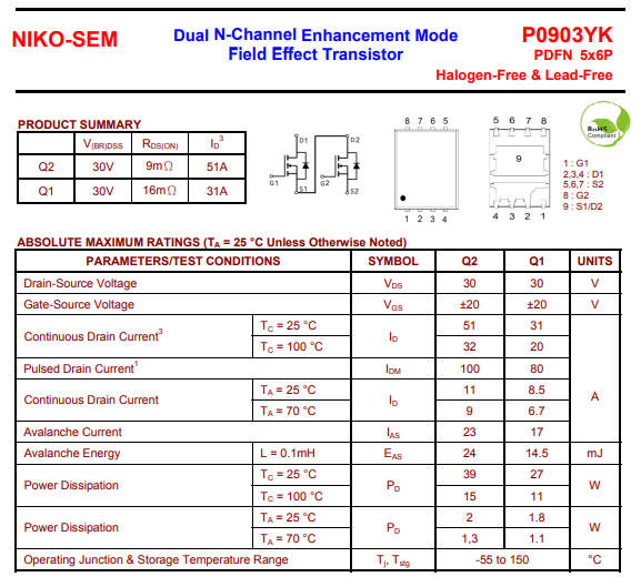
Figure 11: Absolute Maximum Ratings for the P0903YK High and Low Side MOSFET for Phase 1.
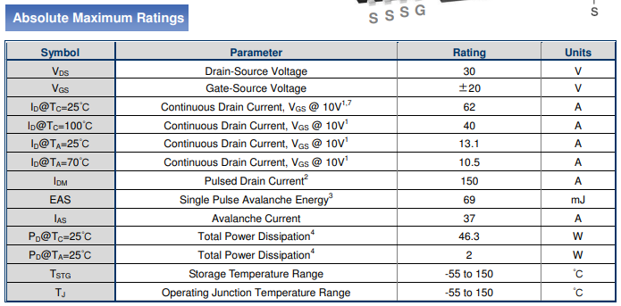
Figure 12: Absolute Maximum Ratings for the M3052M High Side MOSFET for Phase 2.
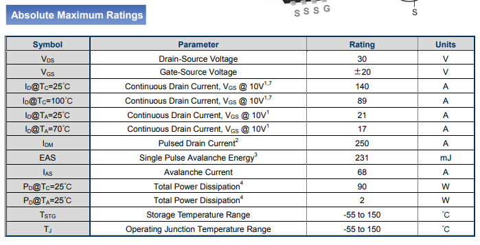
Figure 13: Absolute Maximum Ratings for the M3058M Low Side MOSFET for Phase 2.
Analysis & Conclusion
For a fair comparison, we will focus on the most critical metric for a VRM: Continuous Drain Current (ID), specifically using the Tc=25°C rating as a best-case scenario comparison.
High-Side MOSFET Capability
The High-Side MOSFETs fill the inductor and are most often the bottleneck for total power.
| VRM | Phase | MOSFET | ID (Continuous @ Tc=25°C) |
|---|---|---|---|
| Target (HD 6670) | Phase 1 | M3004D | 55 A |
| Target (HD 6670) | Phase 2 | M3004D | 55 A |
| Donor (R7 240) | Phase 1 | P0903YK (Q1) | 31 A |
| Donor (R7 240) | Phase 2 | M3052M | 62 A |
Low-Side MOSFET Capability
The Low-Side MOSFETs conduct current to ground (completing the circuit) and are critical for efficiency.
| VRM | Phase | MOSFET | ID (Continuous @ Tc=25°C) |
|---|---|---|---|
| Target (HD 6670) | Phase 1 | M3016D | 96 A |
| Target (HD 6670) | Phase 2 | M3016D | 96 A |
| Donor (R7 240) | Phase 1 | P0903YK (Q2) | 51 A |
| Donor (R7 240) | Phase 2 | M3058M | 140 A |
Conclusion
- Low-Side Capability: This is the most interesting finding. The total low-side current handling capability of both VRMs is almost identical (192 A vs. 191 A). This is excellent news, as it indicates the donor VRM’s base efficiency and current handling are perfectly comparable.
- High-Side Capability: The target VRM (HD 6670) has a slightly higher total high-side capability (110 A) compared to the donor VRM (93 A). This means the original VRM was technically “stronger” on paper.
- Asymmetrical Design: The key difference is the donor (R7 240) VRM’s highly asymmetrical design. It’s clear that Phase 2 (140 A Low-Side) is designed to do the heavy lifting, while Phase 1 (51 A Low-Side) acts as a helper. In contrast, the original (HD 6670) VRM had a balanced, symmetrical design (96 A per phase).
Final Verdict: Is it an Upgrade or Downgrade?
Technically, this is a slight downgrade on the high-side, but perfectly matched on the low-side.
However, given that the Radeon R7 240 (where the donor VRM originated) and the Radeon HD 6670 exist in a very similar TDP (Thermal Design Power) class, the donor VRM is 100% suitable as a replacement. The 17A difference in absolute maximum rating (110A vs 93A) on the high-side will not be an issue in real-world operation, as both VRMs were designed to handle a similar load.
The project is deemed safe to proceed.
Integration with the MSI Radeon HD 6670 PCB
This section details the physical modification and the wiring required to integrate the donor VRM into the target GPU.
Modification and Implementation
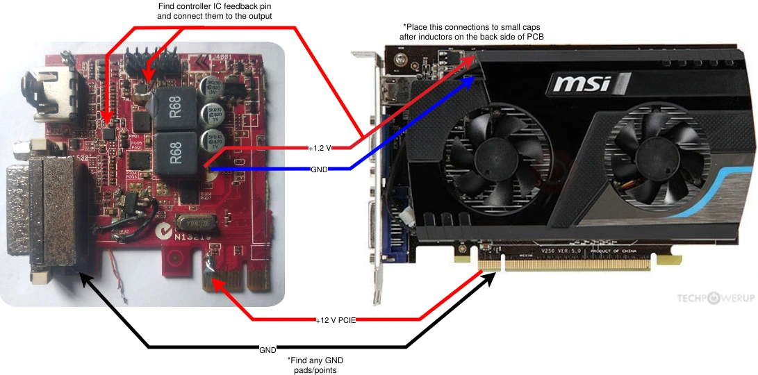
The donor PCB was first prepared by cutting the board to isolate only the VRM circuitry, removing unnecessary components and PCB area. To make the external VRM functional, three critical connections must be established between the donor board and the target HD 6670:
- Main Voltage Output (+1.2V): The output is taken from the pins of the small filter capacitors located immediately after the inductors on the donor board. The default output is approximately 1.2V, though this value can be tuned by modifying the feedback resistor divider for overvolting or undervolting purposes. Due to the high current involved, thick, high-quality copper wire is required to minimize resistance and voltage drop.
- 12V Input Supply: The donor VRM requires a stable 12V supply, which is tapped directly from the PCIe power rail of the target GPU. This 12V rail provides the main power for the MOSFETs and is also stepped down by internal regulators to provide the VCC for the controller ICs.
- Feedback and Monitoring: The Feedback (FB) pin of the VRM controller must be connected to the output rail after the inductor. This connection is vital for the IC to “sense” the output voltage and adjust the PWM signal accordingly. Furthermore, as discussed in the current sensing analysis, the controller relies on this path to monitor current; without this loop, the VRM will enter a fault state and refuse to output any voltage.
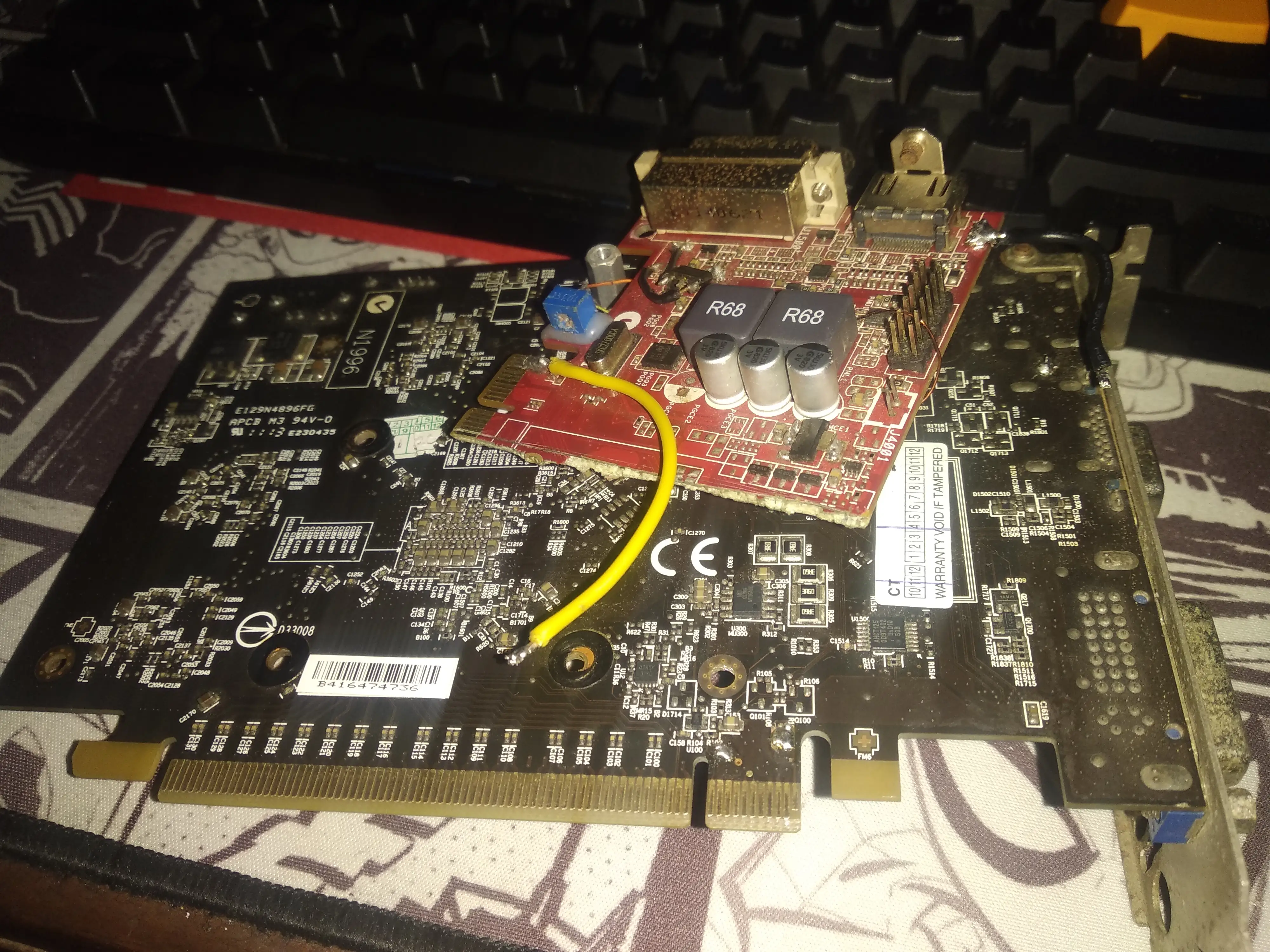
Figure 12: Connecting the +12V power from the target GPU’s PCIe lane to the donor VRM PCB.
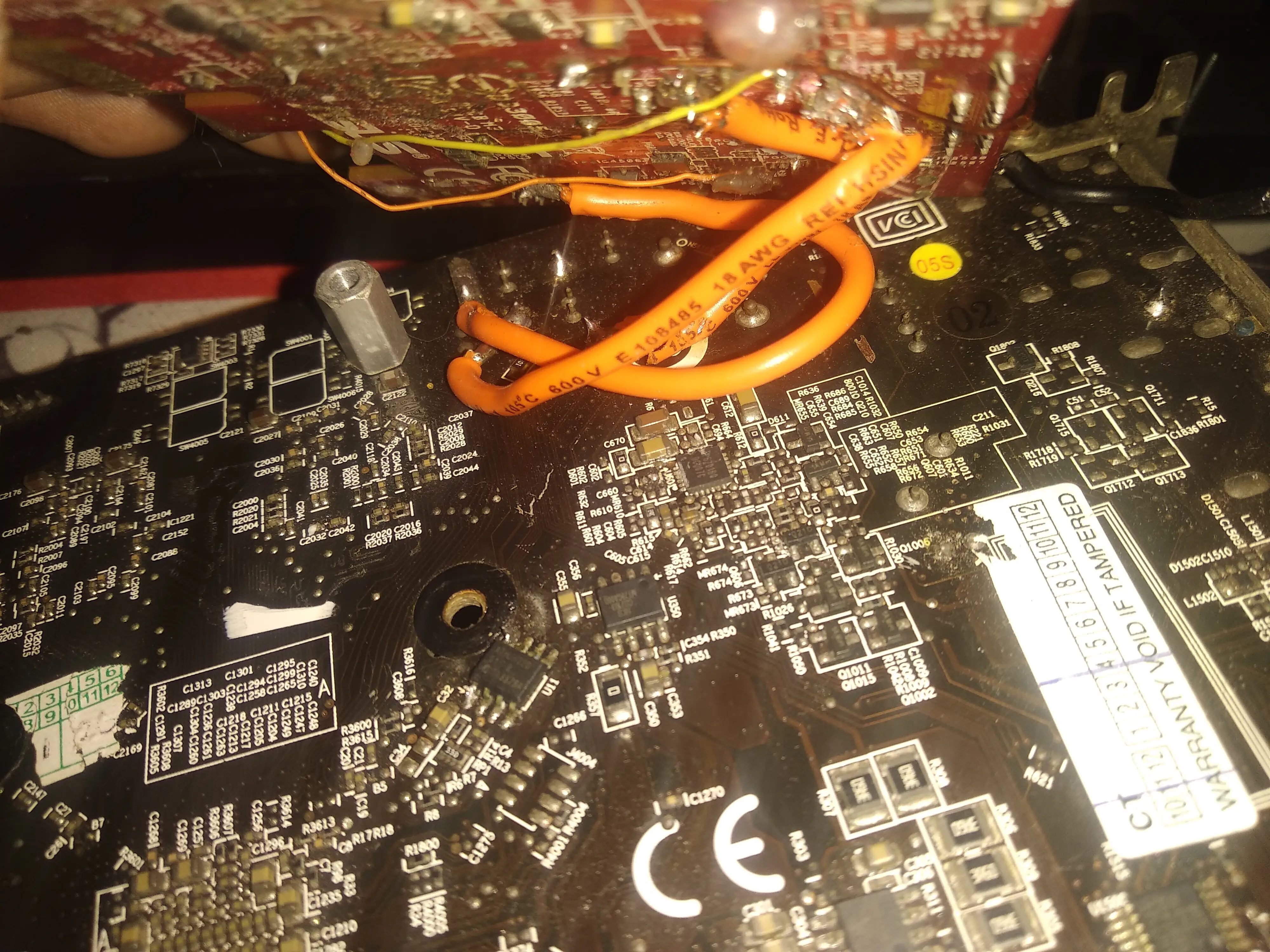
Figure 13: Connecting the +1.2V output and feedback wires to the target VRM’s output stage (backside of the PCB, specifically to the capacitor pins following the inductors).
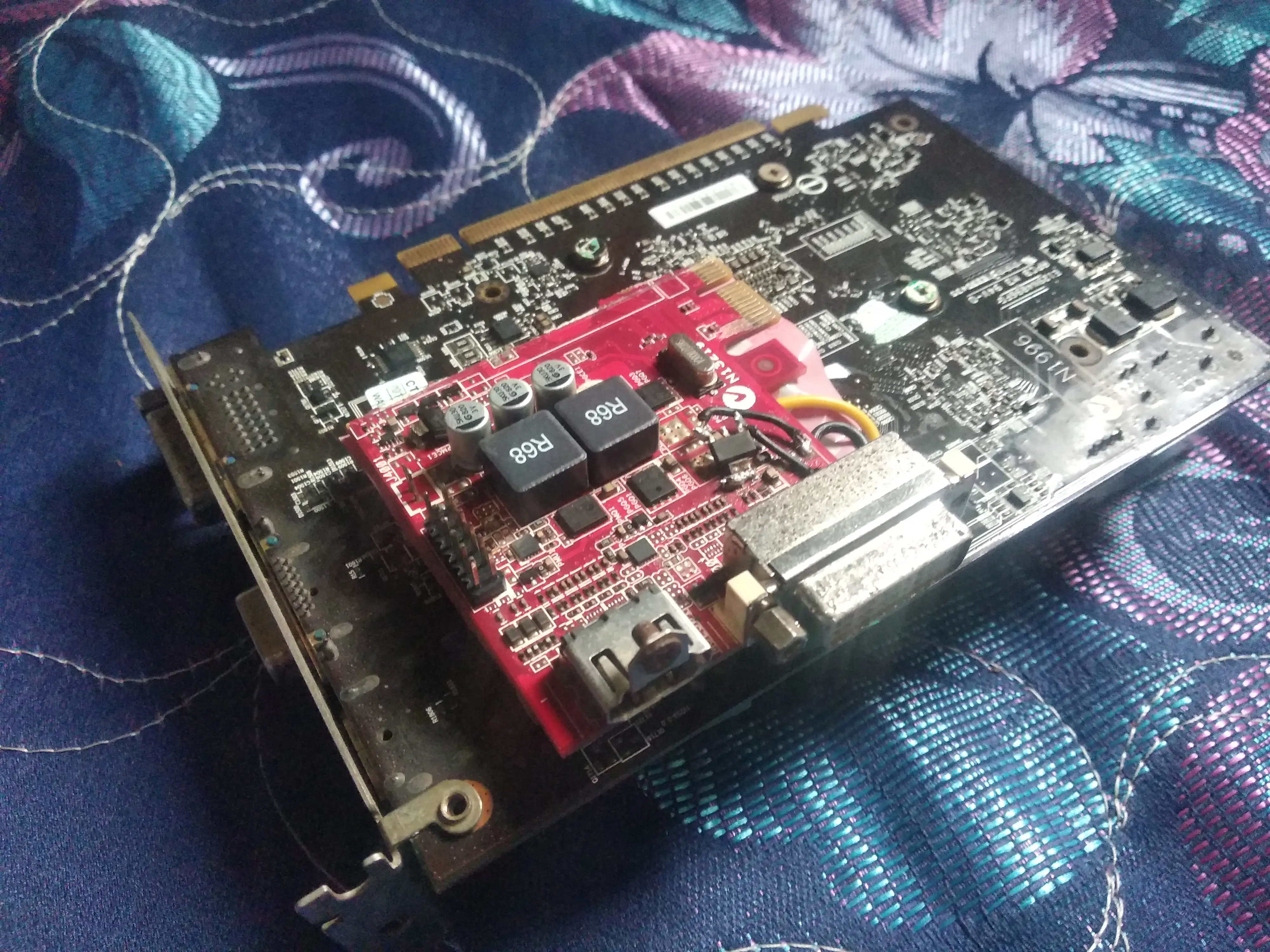
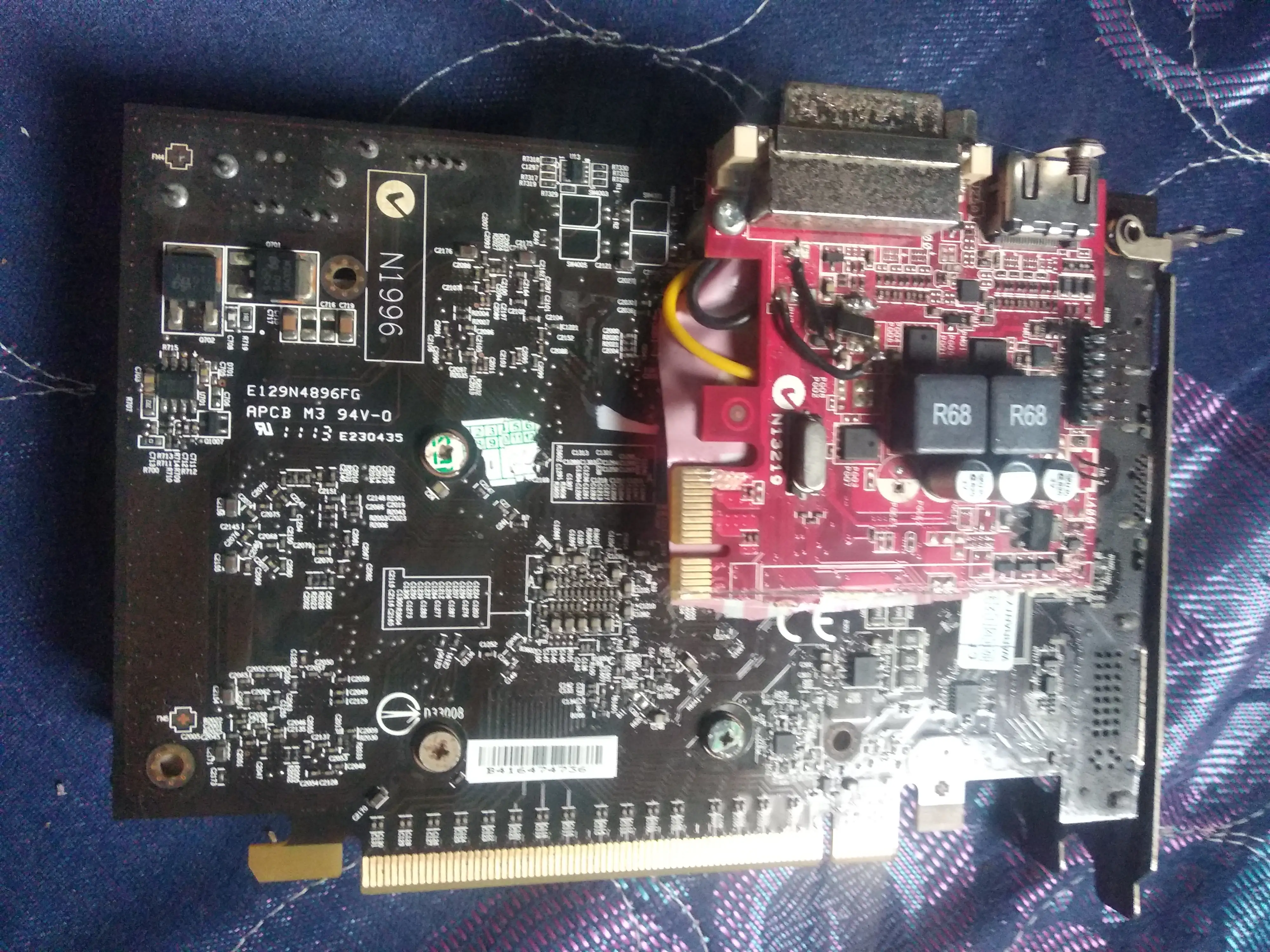
Figure 14: The final assembly showing the donor VRM PCB stacked onto the target GPU using bolts and spacers. Note that the +12V PCIe wire is not shown in this specific frame but is part of the completed circuit.
Changing donor VRM with higher power
After several weeks of operation, the initial donor VRM suffered a failure. The root cause was a dead MOSFET, which forced the system into single-phase mode. This resulted in power delivery that was significantly less stable than the original dual-phase operation; furthermore, the remaining phase was forced to carry the entire load, causing the power inductors to overheat dangerously.
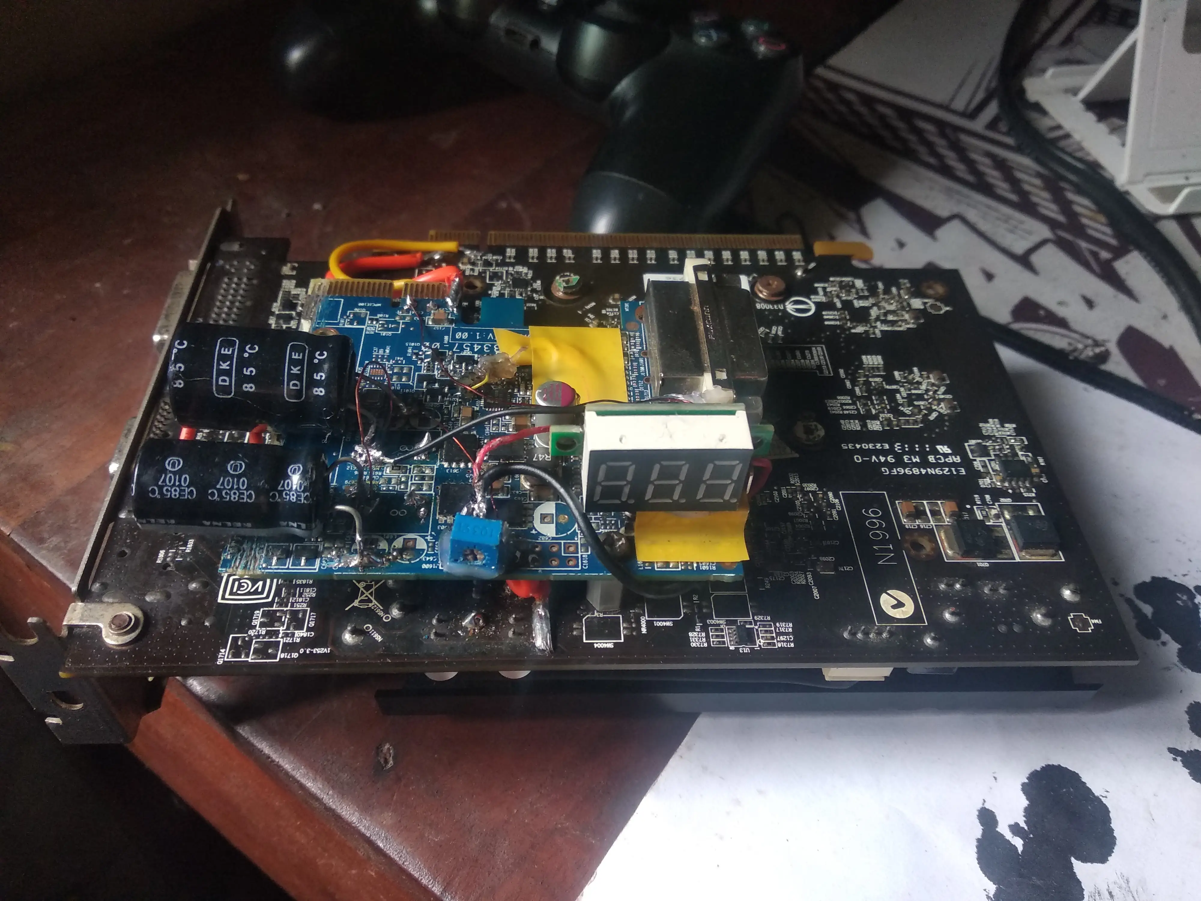
To rectify this, I replaced the failed unit with a more robust VRM salvaged from a Dell Radeon HD 7570. This new donor provides power delivery that is equal to, if not higher than, the target GPU’s original specifications. The modification process remained identical, allowing me to reuse the existing wiring. While the filter capacitors I chose are physically large and arguably overkill, they were what I had available in my parts bin—and in the spirit of hobbyist engineering, “if it works, don’t touch it.”
To enhance the setup, I integrated a mini digital voltmeter to monitor the GPU Vcore in real-time. I also modified the feedback circuit by implementing a voltage divider with a 10kΩ potentiometer. This allows for quick, manual “fine-tuning” of the voltage, making it easy to perform undervolting or overvolting while immediately observing the changes on the display.
Test Result
On progress..